Last updated on March 18th, 2024 at 12:34 pm
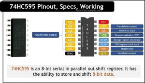
74HC595 is an 8-bit serial in parallel out shift register. It can store and shift 8-bit data. Its main purpose is to take in serial input data and convert it to parallel output so that it can be used by various devices such as LED displays, LCDs, and so on.
For example: If you want to turn ON eight LEDs in a row, you may use eight different pins/signals and turn them all ON one at a time in sequence. Alternatively, you could use a single pin/signal and send in a byte (8 bits) one by one, representing which LEDs should be turned on. A shift register can then receive and store the incoming eight bits before sending the individual bits to the LEDs as parallel output.
Computers, calculators, and other intelligent machines use registers or memory to store data. Typically, there are two such data types: permanent and temporary.
Shift registers are used in these machines to store temporary data. A shift register is a device that uses sequential logic to store and transfer binary data. Shift registers are bidirectional circuits that shift every bit of data from their input to their output on every clock pulse. And 74HC595 is one such Serial to parallel output shift register.
Table of Contents

74HC595 pinout
74HC595 is a 16-pin IC available in through-hole and SMD versions. Its pinout image is given below:

Given below is the pin description of 74HC595 in tabular form:
| No. | Symbol | Name And Function |
|---|---|---|
| 1 | Q1 | Parallel Data Output 1 |
| 2 | Q2 | Parallel Data Output 2 |
| 3 | Q3 | Parallel Data Output 3 |
| 4 | Q4 | Parallel Data Output 4 |
| 5 | Q5 | Parallel Data Output 5 |
| 6 | Q6 | Parallel Data Output 6 |
| 7 | Q7 | Parallel Data Output 7 |
| 8 | GND | Ground(0) |
| 9 | Q7S | Serial Data output |
| 10 | ~MR | Master Reset Input |
| 11 | SH_CP/SRCLK | Shift Register Clock Input |
| 12 | ST_CP/RCLK | Storage Register Clock Input |
| 13 | OE | Output Enable Input |
| 14 | DS | Serial Data Input |
| 15 | Q0 | Parallel Data Output 1 |
| 16 | VCC | Supply Voltage VCC |
The shift register uses 5 control signals for operation:
Serial Data Input (DS) – This pin receives the serial data.
Shift Register Clock Input (SHCP/SRCLK) – This pin controls the data shift(bits) from DS to the shift register. It activates when there is a rising edge at the SH_CP pin.
Storage Register Clock Input (ST_CP/RCLK) – This pin controls the shift of 8-bit data from the shift register to the storage/output register(Q0 – Q7). It activates when there is a rising edge at the ST_CP pin.
Output Enable Input (~OE) – This pin is used to enable or disable the outputs(Q0 – Q7). This is an active low pin meaning when it is at logic ‘0’ the outputs will be enabled.
Master Reset(~MR) – pin is used to reset the shift register. This is also an active low pin which means when it is at logic ‘0’, the shift register resets. Hence this pin is usually connected to +VCC.
How 74HC595 works?

74HC595 is made up of two registers: shift register and storage/output register. Both have an 8-bit width. The first one is in charge of accepting the input data on every positive edge of the clock pulse. The storage register is responsible for delivering the data to the output pins(Q0 -Q7).
Step 1: The eight-bit shift register takes in data from the serial input (DS/SER) on each positive transition of the shift register clock (SH_CP). So 8 clock pulses are required to shift 8-bit data into the register.
Note: When it is low, the reset function (MR) sets all shift register values to zero and is independent of all clocks.
Step 2: The data from the input serial shift register is placed in the output register with a rising pulse at the storage register clock (ST_CP) pin. So one clock pulse is required to transfer the 8-bit data from the first register to the output register(Q0 – Q7).
Note: With the output enable (~OE) asserted low, the 3-state outputs Q0-Q7 become active.
This means that the 74HC595 output will only be updated when latch pin 12 is at the high logic level. The data from the storage register is connected to the 8-output pins, which are connected in parallel and can drive individual loads like LED.
74HC595 timing diagram
Given below is the timing diagram of the IC for a better understanding of its working.

Specifications of 74HC595
- It is an 8-bit SIPO Shift register
- A broad supply voltage range between 2.0 and 6.0 volts
- Sources or sinks with 8 mA at VCC = 4.5V
- Low Power (80uA) Consumption CMOS
- 35mA is the output source/sink current.
- The voltage at the output pins is equal to the operating voltage.
- These Shift Registers are available in a variety of packages, including 16-pin GDIP, PDIP, and PDSO.
- Maximum Clock Frequency: 25Mhz @4.5V
- Can be easily cascaded with additional IC to produce more outputs.
74HC595 datasheet

To download the datasheet of 74HC595, click here.
Applications
- Capture & Hold Logic
- Switches for networks
- Simple Serial to Parallel Data Conversion
- To extend the GPIO pins of the MCU
- In LED matrix or cube projects.
- In Cascading Applications
- Interfacing an LCD
FAQs
What is the operating voltage of 74HC595?
The operating voltage of the 74HC595 is typically around 2V to 6V.
What is 74HC595 used for?
The 74HC595 is mainly used for output expansion in digital circuits, enabling control of multiple output pins using just a few pins on a microcontroller.
What does 74HC595 IC do?
The 74HC595 is an integrated circuit that converts serial data input into parallel output, allowing control of multiple output pins using only a few input pins from a microcontroller or digital device.