Last updated on March 22nd, 2024 at 03:58 pm
ATtiny85 is an 8 bit-RISC-microcontroller that is a part of the AVR family.
ATiny boards were originally developed in 1996 by the company Atmel (AT). But in 2016, this company was acquired by Microchip Technology. ATtiny is also known as TinyAVR and has fewer features, fewer I/O pins, and less memory than other AVR series chips.
These are popular because of their flexibility and small size. With the invention of such small, flexible onboard microcontrollers, electronic projects have become hassle-free and easier to develop than ever before.
Table of Contents
What is ATtiny85?
ATtiny85 is an 8-bit AVR microcontroller based on AVR-enhanced RISC architecture. It has an 8-pin interface (PDIP) and comes in the category of low-power microcontrollers. This microcontroller is designed and manufactured by Microchip.
As per the datasheet, it has 8 KB of flash, an 8-MHz internal RC oscillator that can be used as the default clock & 512 bytes of EEPROM and SRAM.
In achieving a throughput of 20 MIPS, it takes 20 MHz and operates between 2.7 and 5.5V.
It also has two 8-bit timers or counters, one high-speed, with four pulse-width modulations (PWM) outputs, and a four-channel 10-bit ADC.
An ADC converter with a 10-bit & programmable watchdog timer is added to the device which makes it suitable for resetting the device in case it gets stuck in an infinite loop and sensor interfacing.
Although it consists of 8 pins only, it can perform almost every function that a simple microcontroller can do. We will get a better idea of its functionality in the pinout specification.
What does the number 85 in ATtiny85 represent?
In the ATtiny series, the first digit that comes after ATtiny represents the flash memory in kibibyte (KiB). Thus, an ATtiny85 consists of 8KiB flash memory.
The second digit represents the model type. You can expect more powerful and newer models to have higher numbers. Here you can see that ATtiny85 is a 2005 model.

- ★Support for the Ar-duino IDE 1.0+ (OSX/Win/Linux)
- ★Power via USB or External Source – 5v or 7-35v (automatic selection)
Specifications of ATtiny85

The features and characteristics of ATtiny85 are summarized in the table below:
| SPECIFICATION | DESCRIPTION |
| CPU Architecture | 8 bit (RISC) |
| EEPROM | 512 Bytes of In-System Programmable EEPROM |
| CPU (Speed) | 1 MIPS@1MHz |
| RAM | 512 Bytes (on Internal SRAM) |
| Total Number of Pins | 8 |
| No. of I/O Pins (Programmable) | 6 |
| Operating Voltage | +2.7V to +5.5V (For ATtiny85) (+6.0V is absolute maximum supply voltage) 1.8V to +5.5V (For ATtiny85V) |
| Operating Temperature | -55ºC to +125ºC |
| External Oscillator | For ATtiny85V: 0-10MHz For ATtiny85: 0-20MHz |
| Internal Oscillator | 0-8MHz (Calibrated Internal R-C Oscillator) |
| Maximum DC Current through Vcc and GND pins | 200 mA |
| Maximum DC Current per I/O Pin | 40 mA |
| ADC Feature | 4 channels,10-bit resolution ADC |
| PWM outputs | 4 |
| Communication Interface | Master/Slave SPI Serial Interface(5,6,7 PINS) – can be used for programming this controller. Universal Serial Interface (5,6,7 PINS) – can be used for communicating with other controllers I2C or 2-wire Serial Interface(5,7 PINS)- can be used to connect peripheral devices and sensors |
| UART Interface | NA |
| Timer Module | Two 8-bit counter |
| Analog Comparators | 1 |
| Program Lock | Available |
| Program Memory or Flash memory size | 8 Kbytes [10,000 write/erase cycles] |
| Power Save Modes | 3 modes [Idle, ADC Noise Reduction, Power-down] |
| Watchdog Timer | Available |
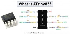
ATtiny85 pinout

The ATtiny85 pinout is discussed below:
Pin 1 (PB5)- It is for an analog pin ADC0 and is used for analog sensors.
Pin2 (PB3)- It is for an analog pin ADC3 and also for crystal oscillator XTAL1.
Pin3 (PB4)- It is for analog pin ADC2 and is also used for crystal oscillator XTAL2.
Pin4 (GND)- It should be connected to the Ground.
Pin5 (PB0)- This pin is used as MOSI (Master Out Slave In). It can be used as a master line for sending data to the peripherals for SPI communication and SDA for I2C Communication.
Pin6 (PB1)- This pin is used as MISO(Master In Slave Out). It can be used as a Slave line for sending data to the master.
Pin 7 (PB2)- This can be used as SCK for SPI Communication and SCL for I2C Communication.
Pin 8 (Vcc)- It is used as a Vcc Pin & 5V is applied to it.
Detailed description of the pins
Power
ATtiny85 has two power pins. One is used for the power supply while the other connects to the ground. The power supply to the ATtiny must not exceed the rated voltage.
Pin8– Vcc
Pin4-GND
Oscillator/Clock
Attiny85 has an 8MHz internal clock and its clock value varies from 0-8MHz. But it can expand its oscillator up to 20MHz. So, to increase the oscillator value, it should be connected to the oscillator pins.
GPIO2– XTAL1/CLKI
GPIO3-XTAL2/CLKO
Digital input/output
In ATtiny85, any pin can be used for input and output signal but, it should be mentioned in the program before. These pins are used as bidirectional Input/Output. Except for the power supply pin, any pin we can use for Input/Output purposes.
GPIO5- PB0
GPIO6- PB1
GPIO7- PB2
GPIO2- PB3
GPIO3- PB4
GPIO1- PB5
Interrupt
ATtiny85 has one interrupt pin. This pin can be controlled by any sensor output, or manually via a button.
GPIO7- INT0
SPI
The SPI pins on Attiny85 are:
GPIO5- MOSI
GPIO6-MISO
GPIO7- SCK
GPIO1- Debugging wire(DW)
- MOSI is used to send the data
- MISO is used for receiving the data
- SCK for the clock
- DW for programming
I2C
The I2C communication protocol is also available in Attiny85. In this protocol, data is sent and received by a single line while another line sends a clock pulse through which data is kept in sync by the time. The I2C pins are:
GPIO5- SDA(Data)
GPIO7- SCL(Clock)
Timer
ATtiny85 consists of two timers, i.e., Timer 0 and Timer 1, that are used to count the clock pulses. These two clocks work according to the internal clock, but Timer 0 can be operated by an external clock pulse.
These both Timers consist of 8-bit. The timer pins are:
GPIO7-Timer 0
Counter/Timer and PWM
PWM stands for Pulse Width Modulation. The Attiny85 consists of four PWM channels.
In Attiny85, there are some special pins and with the combinations of the internal PWM signal input, it can be used to drive the external power efficiently.
These pins function according to a particular time which is known as Dead Time Generator. The timer counts the value and compares its value until it reaches zero.
In ATtiny85, Timer 0 and Timer1 are used to count two dead generator values and the output signal comes in the non-overlapping form.
GPIO-OC1B
GPIO-OC1B’
GPIO-OC0B
GPIO-OC0A
GPIO-OC1A
GPIO-OC1A’
Analog Comparator
Attiny85 has an internal analog comparator through which an analog signal can be compared in the form of inverted and non–inverted. Within the register, the output that comes from the comparison is stored and can be used for further purposes. Analog comparator pins that are available in Attiny85:
GPIO5-AIN0
GPIO6-AIN1
Analog to digital converter
There are four analog input channels available in Attiny85.
Analog input is changed into a 10-bit digital output. With the speed of 65-260us, ATtiny85 converts the analog data which is sufficient to update the system at every second.
Analog input voltage is determined as per the power supply voltage which may cause the possibility of errors in external devices. An analog reference pin is used to eliminate this error. Due to this, the system gets information about the voltage maximum and minimum level to the voltage reference given to it. The reference voltage and an analog input voltage should not cross the limit of the actual voltage power handled by the controller. Analog pins are:
GPIO1-ADC0
GPIO7-ADC1
GPIO3-ADC2
GPIO2-ADC3
GPIO5-Vref
Reset
Attiny85 has an external and internal reset. This can be reset on a particular condition applied by the program or can be done from an external pin.
What can ATtiny85 be used for?
Atttiny85 can perform several functions on a single chip as some of its pins can do multiple functions. Some of the main functions are described below.
Timers
The chip has two timers that help in generating a delay in the running process of certain functions when they perform in timer mode. The timer mode increases the instruction cycle.
While in the counter mode, these timers are used to count the number of intervals on a specific function inside the controller. The counter mode is used to increase the rising and falling edge of the pin in it.
Peripheral interface (SPI) communication

The serial peripheral interface (SPI) is used for communicating microcontrollers with other peripheral devices like sensors, SD cards, etc.
It consists of a separate clock and data lines with the addition of a select line to choose the required device to build communication. This allows both connected devices to layout the same communication path following one communication protocol.
I2C communication
I2C protocol is a 2-wire protocol, incorporated in the device to connect low-speed devices like DAC converters & ADC, I/O interfaces & microcontrollers.
Serial Data (SDA) & Serial Clock (SCL) are the two wires and are the main part of this communication protocol.
Brown out reset (BOR)
This function helps reset the controller once Vdd (voltage supply) comes below a brownout threshold voltage. The multiple voltage ranges are provided once the power drops below the voltage supply line.
Interrupt
This function works on a priority basis. It puts the main function on hold and executes the required instructions that are necessary at that time. Once it is executed, the executing code puts the controller again to the main program.
ADC
In this device, the ADC module is a valuable feature that helps to make it more compatible with the sensors. It is a 10-bit module that consists of 4 channels which are lesser than the number of modules introduced by Microchip (7 or 12 channels).
What is the memory layout of ATtiny85?

Atttiny85 memory is based on Atmel’s high-density technology that is non-volatile.
Through SPI serial interface, the Program Memory can be reprogrammed in two ways.
- On-chip boot code
- Non-volatile memory programmer
The execution of the main program mainly happens inside the CPU which plays a vital role in accessing memories and performing calculations.
This module falls under the category of AVR controllers and has separate reserved locations for both data & program memory.
Program memory (ROM)
Program memory is a reprogrammable flash memory.
The Flash memory has 8k memory space and consists of memory endurance approx. 10,000 write/erase cycle which means you can erase and write the instructions 10,000 times on this board.
On the flash memory, the available program counter is 12 bits wide which can address 4096 program memory locations.
Data memory (RAM)
The data memory has a memory space of 512 bytes and it reserves the memory locations in three ways, i.e.,
- starting 32 locations to access the file register
- next 64 locations: reserved for standard I/O memory
- remaining are used for internal data- SRAM.
Five addressing modes categorize the data memory.
- Direct
- Indirect
- Indirect with Displacement
- Indirect with Pre-decrement
- Indirect with Post-increment
The registers from R26 to R31 in the Register File refer to the pointer registers having indirect addressing. The entire data space is covered in the direct addressing.
The Indirect with Displacement covers 63 address locations using a base address that can be accessed by the Y or Z register.
When indirect addressing modes are layered with both post-increment and pre-decrement, the address registers X, Y, and Z increment and decrement at regular intervals.
ATtiny85 block diagram

In visualizing the main function available in the controllers, we need to study block diagrams and have to find how each component is connected. The figure below shows the block diagram of ATtiny85.
Programming
A compiler is always needed to program the Atmel microcontroller.
- Atmel Studio
- Mikro C for AVR
- AVR – GCCAVR – (toolchain for Linux & Windows)
The IDE programmer used to program Arduino can also be used to program the Attiny85.
ATtiny85 works similar to other microcontrollers and executes the application program saved in its memory. Without programming, the controller simply stays idle.
Equivalent of ATtiny85
ATtiny25 and ATtiny45 are the alternatives to ATtiny85. But, the flash memory, SRAM, and EEPROM are different in both of them.
What are the packages available in ATtiny85?
There are two types of packages available in ATtiny85. These are the SMD package and DIP package.
Surface-mounted device (SMD)

Dual In-line package (DIP)

What are the applications of ATtiny85?
ATiny85 is widely used in areas where there is a requirement to embed small-sized chips. Some of its applications are:
- In real-time applications related to industrial automation.
- It can be applied in robotics.
- IoT based projects
- In aeronautical technology, there is a wide range of AVR controllers.
- Power monitoring and management systems.
- Measurement in Analog signals and manipulations.
- Coffee machines, vending machines, and other embedded systems.
- Multifunctional display units.
- Peripheral interface and machine-controlling systems
- Solar applications and Weather sensor systems
- Wireless communications
- Security based applications
- Medical & health equipment
- Automobiles
Conclusion
ATtiny85 is used in many embedded projects and when programmed using Arduino IDE, it can do wonders by performing several functions. It has fewer pins, an economical price, and the overall power consumption is low.
So, overall the ATtiny85 is efficient and value-for-money, which meets all your technical demands.
FAQs
Is ATtiny a microcontroller?
Yes, ATtiny is a microcontroller. It’s a subfamily of the popular AVR microcontrollers produced by Microchip Technology.
What is the speed of ATtiny85?
The ATtiny85 can operate at a variety of speeds, but its default speed is 1MHz.
Does ATtiny85 have analog input?
The ATtiny85 does not have dedicated analog input pins in the traditional sense. However, it can perform basic analog-to-digital conversion (ADC) using some of its digital I/O pins.
Can de input pins handle negative voltage through the ADC?
It cannot unless you interpose a bridge rectifier before the ADC.
Any sample code??