Last updated on March 30th, 2024 at 06:23 pm
A diode is an electronic device that allows current to flow easily in one direction but restricts current flow in the opposite direction. Semiconductor diodes are widely used in modern electronic circuits for rectification, voltage regulation, signal modulation, and more.
This blog post is all about diode- definition, its working, types, and applications.
Table of Contents
Diodes are also known as Rectifiers. The term diode is reserved for small signal devices which consume a maximum current of 1 A, while the term rectifier is used for power devices.

Given above is a rectifier circuit. A rectifier circuit converts the AC voltage to stable DC voltage with the help of diodes and filters. Diodes used in this circuit convert the input AC waveform into fluctuating DC waveform. This fluctuating DC waveform is then made stable using a capacitor as a filter.
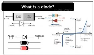
Symbol
The standard symbol for diodes is given below. Two terminals of the diode are the anode and cathode. The arrowhead represents the flow of current during the forward bias.

Working principle
A diode can easily allow or block the flow of electric current based on the way it is connected in a circuit. Consider two cases to understand the principle in detail.
Case 1: When the anode is connected to the positive pole of the battery

In this orientation, the diode is forward biased. The diode offers little resistance to the electric current in this state, and hence the bulb glows which is connected to the circuit.
Case 2: When the anode is connected to the negative pole of the battery

In this orientation, the diode is reverse biased. In this state, the diode offers very high resistance to the flow of electric current. The diode does not conduct, due to which the bulb connected to the circuit remains OFF.
Note: A diode conducts when it is connected in a particular way (forward-biased) in a circuit. Hence diode is a type of unilateral device.
Water-flow analogy
The unilateral behavior of the diode can be understood with the water-flow analogy. Consider a gate attached with a spring mechanism as shown in the figure below.
Case 1: When water flow is from left to right

When the water pressure exceeds a certain threshold, it pushes the gate, and the water flows easily. This condition is similar to the forward biasing of the diode.
Case 2: When water flow is from right to left

In this case, irrespective of the water pressure, the gate does not open. Thus, no water flows in this case. This condition is similar to the reverse biasing of the diode.

Given above is the PCB board of an LED bulb. Several LEDs are connected together in order to output high-intensity light. Please note that an LED works on DC voltage only but the LED bulb is AC. The circuit inside the bulb converts the input AC voltage to a suitable DC voltage for the LEDs.
Construction
A PN Junction diode is a two-terminal semiconductor device whose one side is doped with P-type material (acceptor) and another with N-type material (donors) as shown in the figure below. Electrons and holes are the majority carriers in the N-type and P-type regions respectively.

The formation of the depletion region
These electrons in the N region and holes in the P region recombine due to concentration differences. This results in positive ions in the N region and negative ions in the P region. These ions are collected at the junction. And this region is known as the depletion region.
Bias is the external voltage applied to the PN Junction. When no voltage is applied to the diode then it is zero bias. Depending upon the voltage potential applied to the diode, it is operated in two modes; forward biased mode and reverse biased mode.
Diffusion current
The flow of charge carriers across the junction area is known as diffusion. Hence the current at no bias condition is known as diffusion current.
Barrier potential
The electric field formed in the depletion region acts as a barrier. External energy must be applied to get the electrons to move across the barrier of the electric field. The potential difference required to move the electrons through the electric field is called the barrier potential.
The barrier potential of a P-N junction depends on the type of semiconductor material, amount of doping, and temperature. This is approximately 0.7V for silicon and 0.3 V for germanium.
Working
Forward biased
It is the condition where the positive terminal of the battery is connected to the P-type material and the negative terminal of the battery is connected to the N-type material of the diode. The figure below shows a diode in the forward-biased mode.

The electric field created by the applied voltage forces the electrons in the n-side of the diode to move towards the p-side, while also forcing the holes in the p-side to move towards the n-side. This movement of electrons and holes creates a current through the diode. In this condition, the width of the depletion region decreases.
Knee voltage
As the supply voltage increases above barrier potential (the knee voltage), the majority of charge carriers flow through the circuit and it makes the diode conducting.
Reverse biased
In reverse biased conditions, the positive terminal of the battery is connected to the N region, and the negative terminal of the battery is connected to the P region. A diode in reverse bias mode is shown in the figure below.

In this case, the negative terminal of the battery attracts the holes in the p-side away from the edge of the junction barrier. On the other hand, the positive terminal attracts the electrons in the n-side away from the edge of the barrier. This prevents current from flowing through the diode, as there are no carriers available to carry it, and hence the width of the depletion layer increases.
Leakage current and breakdown voltage
Usually, a small current flows when a diode is reverse-biased, known as the leakage current. This is due to the movement of minority charge carriers across the junction. However, at normal operating temperatures, this small current may be neglected.
Graphical representation
The PN junction diode offers very little resistance to current flow in the forward-bias direction but maximum resistance to current flow when reverse biased. A good way of illustrating this point is by plotting a graph of the applied voltage versus the measured current. The figure below shows a plot of this voltage-current relationship (characteristic curve) for a typical PN junction diode.

Different types of diode
Different types of diodes are available in the market, which come in handy in various applications. Some of them are listed below.
- Light Emitting Diode(LED)
- Schottky
- Shockley
- Laser
- Avalanche
- Zener
- Photodiode
- Varactor
- Tunnel