Last updated on March 28th, 2024 at 06:15 pm
A Schottky diode is a special type of semiconductor diode that has a very low voltage drop and is used for high-speed switching applications. The junction is formed with a metal and a semiconductor. In this article, we will discuss the applications, and working of this diode. We will also learn how it is different from a PN junction diode.
The term “Schottky” comes from the German physicist Julius Schottky, who first described this effect in metal-semiconductor junctions.
Table of Contents
Symbol
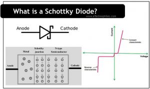
The symbol is shown in the figure below. The anode is the metal and the cathode is the semiconductor in the metal-semiconductor junction.

It is also known by the names of hot-carrier diode, Schottky barrier diode, surface barrier diode, majority carrier device, hot-electron diode, or hot carrier diode.
How are Schottky diodes manufactured?
While traditional diodes are made from two pieces of semiconductor material (one n-type and one p-type), these are only made from one piece of n-type material. This material is typically alloyed with another metal, such as aluminum or platinum.
The resulting junction between the metal and semiconductor material is what gives the Schottky diode its low forward voltage drop.
Additionally, since there is no p-type material involved, there is no depletion region and electron injection is much more efficient than in traditional diodes. As a result, Schottky diodes have faster-switching speeds than traditional diodes.
Note: Schottky barriers can form in both n- and p-type semiconductors. The forward voltage is often much lower for p-type semiconductors. It cannot be too low. Because the reverse leakage current increases significantly by lowering the forward voltage. So N-type silicon is usually used for semiconductors. The cathode of the diode is an n-type semiconductor, and the metal side serves as the anode.
The schottky barrier helps in both very fast switching and low forward voltage drop. The typical value of forwarding voltage is about 0.5–0.7 V.
What is the Schottky barrier?

A depletion layer developed at the intersection of an n-type semiconductor and metal is a Schottky barrier. The width of the depletion layer depends on the concentration of semiconductors and the combination of metals used.
Working
Forward biased condition
In forward-biased conditions, metal is connected to the positive terminal of the battery, and n-type semiconductor material is connected to the negative terminal of the battery.
When voltage is applied, free electrons are generated in metal and semiconductors. If the applied voltage is greater than 0.2 V to 0.3 V these free electrons gain potential energy to overcome the Schottky barrier. The built-in potential is opposed by the voltage, which facilitates smooth current passage.
Thus the Schottky diode starts to conduct electric current. As voltage increases, the depletion layer becomes thin and finally vanishes.

Reverse biased condition
In reverse biased conditions, metal is connected to the negative terminal of the battery, and n-type semiconductor material is connected to the positive terminal of the battery.
As voltage is applied, the width of the depletion layer will increase. Thus no electric current flows through the Schottky diode. Due to thermal excitation, a small leakage current flows through the diode.
There will be a rapid rise in the electric current if the reverse bias voltage is significantly increased. That is, the depletion region will break down and damage the device
The majority of charge carriers present in the Schottky diode are electrons.
V – I characteristics
The V(voltage)-I(Current) characteristics are shown in the figure below. The V-I characteristics of the PN junction diode and Schottky diode are identical.

The forward voltage drop of the Schottky diode is low as compared to PN Junction diodes. Similarly, the reverse saturation current in a Schottky diode happens at a very low voltage.
Differences between PN junction diode and Schottky diode
They both have similar VI characteristics. But there are some parameters in which they differ a lot. Some of them are listed below.
| Parameters | PN Junction Diode | Schottky Diode |
| Switching Speed | Low | High |
| Unwanted Noise | High | Low |
| Voltage Drop | 0.6-0.7V | 0.2-0.3V |
| Junction Formation | The junction is formed by a p-type and n-type semiconductor | The junction is formed by a metal and n-type semiconductor |
| Reverse Recovery time | Slow ( i.e. change from ON to OFF state is slow). | Fast ( i.e. change from ON to OFF state is fast). |
| Depletion region | The depletion region is present | Negligible depletion region |
| Current Density | Low as compared to Schottky diodes | High current density |
Applications
It is typically used in high-speed switching applications, rectifiers, and voltage regulators.
- The Schottky diode has a lower forward voltage drop than a conventional diode, making it ideal for use in power supplies and solar inverters.
- The Schottky diode can handle higher current levels than a conventional diode, making it well suited for use in power supplies and motor controllers.
- The Schottky diode’s reverse recovery time is much shorter than a conventional diode, making it ideal for use in high-speed switching applications.
Advantages
- High efficiency
- Can operate in high frequencies
- Low unwanted noise
- Low junction capacitance due to the thin depletion region
- Fast switching speed (change from ON to OFF state is fast)
- Low forward voltage drop. (0.2 to 0.3 for schottky diode and 0.6V -0.7V for silicon diodes)
Limitations
- Relatively high reverse leakage current
- Thermal instability: Reverse leakage current increases with temperature
FAQs
What is a Schottky diode used for?
It is used primarily for its fast switching and low voltage drop characteristics, making it suitable for applications such as rectification, voltage clamping, and reverse polarity protection in electronic circuits.
Which metal is used in the Schottky diode?
It typically uses a metal-semiconductor junction, where the metal component is often made of materials like platinum (Pt), tungsten (W), or titanium (Ti).
What is the main advantage of a Schottky diode?
The main advantage is their lower forward voltage drop compared to conventional PN junction diodes. This results in faster switching speeds, reduced power losses, and improved efficiency in electronic circuits.